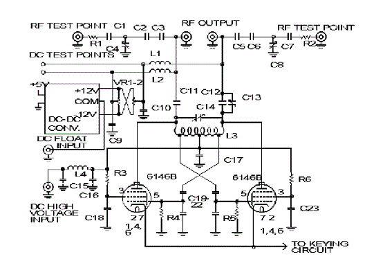
RF Section Schematic
A better copy of the schematic saved in different formats can be downloaded for viewing and printing using different software.
A word of warning, if you download one of these other schematic files, be sure to save them with the proper 3 letter extention. The program may assign a different extention so be sure to change it to the proper one!!
RFSCH.DXF this is a somewhat universal exchange format that can be read by a number of graphics
programs.
RFSCH.SKD this is the original drawing file in AutoSketch format
Note: some of the RF parts are difficult to find commercially. Click on the * to link to a page with addresses and part numbers for possible sources for these hard to get parts.
R1, 2 = 390 ohm, 5%, 1/4 W, carbon composition or equivalent
R3, 6 = 25 K, 10 W, wire wound is OK,
R4, 5 = 75 K, 5%, 1/2 W, carbon composition or equivalent.
Note: C1-C8 are for the RF test point output and may have to be adjusted per the layout. Also, these values were selected for use with a 4' long RG-58 test cable connected between the RF generator and an oscilloscope high impedance input.
C1,C7 = 24 pF silver mica, 500 V
C2,3,5,6 =8 pF silver mica, 500 V
* C4, 8 = 2 to 26 pF, 250 V chassis mount air variable. Note, tuning shaft is grounded.
C9,10,15-18,23 = .01 uF, 1 kV ceramic bypass caps. Keep leads short.
C11 = 1200 pF, 3 kV disc ceramic
C12 = 1000 pF, 3 kV disc ceramic
* C13 = 36 to 200 pF, 1500 V, air variable
C19-22 = 33 pF, 1 kV, disc ceramic
* DC to DC converter
* L1,2 = 2.5 mH, 160 mA RF choke
L3 = RF tank coil. See text below for details:
See the photo gallery for photographs of the coil.
We made two RF tank.
Low frequency coil:
Approximate frequency range: 1 MHz - 14 MHz
Diameter = approx. 2 inches (5 cm)
Length = approx. 7 inches (17.7 cm)
Number turns = approx. 42 turns
High frequency coil:
Approximate frequency range = 10 MHz - 25 MHz
Diameter = approximately 1 inch (2.5 cm)
Length = approximately 7 inches (17.7 cm)
Number turns = approx. 14 turns
Coils are made with #12 AWG solid copper wire. The coil form is made with two pieces of flat, 1/8 thick (317 mm) plastic that are notched and fit slid together at right angles. The coil of wire is first wrapped around a pipe or dowel of appropriate diameter to perform the coil. Holes are drilled in the plastic form at the appropriate spacing and the coil is threaded into the holes around the form. This sounds rather awkward, however it works very well and is extremely easy to make the coils. The holes for the wire should allow the wire to loosely travel through. If the holes are too small, it will be very difficult to thread the coil. This will take a bit of trial and error to find the right size for your situation.
The coils are made to be removable and are held in place with a screw on each end that screw to plastic stands. When the coil is in place, a female banana plug soldered to the center of the coil mates with a male jack mounted on a standoff on the chassis.
CIRCUIT DESCRIPTION
The basic circuit consists of two RF tubes cross-connected in push pull configuration. The main feature of the design is that is a high voltage oscillator as opposed to a low voltage oscillator with an amplifier. Also, the output IS the voltage across the oscillator tank circuit.
High voltage DC (the B+ or "plate" voltage) is coupled from an external power supply through an mV connector on the side of the RF generator. An mV connector is a high voltage version of a standard NBC connector and is used to provide a coaxial shielded high voltage input to the generator yet keep it from accidentally being connected to the lower voltage NBC connectors which connect to components that could be damaged with the high B+ voltage.
The B+ is decoupled from the RF thought a RF filter, L4 and C15 and C16. This blocks RF from getting back down the power line to the DC supply. B+ is connected to a standoff in the chassis which has a high voltage bypass capacitor very near to it. Connected to this point are the two screen resistors, R3 and R6. These are 25K power resistors and get warm to the touch when in use. They limit the screen current and voltage. Near pin 3, the screen pin, is a bypass capacitor to further decouple any RF. The grid bias (sometimes called the grid leak resistor) is a 75 K, 1/2W non-wire-wound resistor. Keep the lead length as short as possible.
B+ is connected to the center tap of the tank inductor, L3. This is done by a connector soldered to the center of the coil and a mating connector on a standoff on the chassis. An RF bypass capacitor, C17, is mounted as close as possible to this connector. It is important to have the DC applied to the center tap of the inductor as free of RF as possible and good bypassing at this point is vital. If removable inductors are not required, solder directly to the center of the coil a 0.1 uF 1 kV capacitor and ground the other end of the capacitor. Keep the leads as short as possible and if one lead must be long and the other short, make the lead to the coil the short one.
The plates receive B+ by way of the DC path through the coil, which, along with C14 forms a resonant tank circuit. The RF voltage at the ends of a tank circuit are 180 degrees out of phase and, since the center tap is connected to B+, the ends of the tank circuit swing about this B+ voltage and are 180 degrees out of phase. This means, when one plate is going in the positive direction the other plate goes in the negative direction. When operating optimally, the plate voltage will swing to as low as 0 Volts and as high as twice the B+ voltage. Since the two plates are out of phase and are connected to the output, that means the peak to peak voltage between the two output terminals will be twice the applied B+ voltage. If B+ is 600 V the breakdown voltage of the load must be greater than 1200 V.
Feedback to the grids is by way of taps part way down from the plate taps. Taps at a voltage point that is lower than the plate voltage are connected to the opposite grids. They are AC coupled and voltage divided by C19 - C 22. The AC signal applied to the opposite grids sustains oscillation. The grid tap locations are not critical, in practice they should be two or three turns from the plate taps.
The output is taken from across the tank circuit. It is AC coupled to block the B+ DC component. Two output phases are connected to a low DC voltage source which drives a bridge circuit consisting of the ganged pot VR1-2. When the pot is in the mid position the voltage applied to the two outputs will be 0 VDC (i.e. no difference potential). The pot is adjusted in one direction or the other to adjust the magnitude and polarity of the voltage applied to the two output terminals. This gives a low DC voltage between the two output terminals that is independent of the RF voltage.
The low voltage supply we used is a DC to DC converter that converts +5V DC to +/- 12 VDC and the output ground or common is not connected to the +5V ground. Since we had a +5V available from the keying circuit, we decided to take advantage of it. If no keying circuit is used, it may be easier to use a pair of batteries in a bridge circuit similar to the one we used, however, one must consider the life of the batteries.
The low voltage power supply has a floating ground and this ground can be connected to an external power supply to apply a common DC voltage to the output. This is the DC float voltage. This power supply is connected to the output through a DC path that blocks the RF consisting of L1, L2 and C9 and C10.
The output is connected to two test circuits. One allows the DC component of the output to be measured from the front panel. The output of the DC to DC converter is connected to a front panel test point. This gives an RF-free measurement of the DC on the output. It can be measured with a simple DVM or an oscilloscope.
The RF can also be measured from the front panel, however, since the output can be a very high voltage and since the nature of this circuit is such that anything attached to the output will affect the circuit, the output test point has associated with it a 100:1 attenuator. This reduces the output at the test point by a factor of 100 which makes the front panel test point much safer and it also reduces the loading of the test equipment on the output by a factor of 100. In practice, if the RF output test point is shorted, there is almost no difference detectable on the output. The RF output test point is a front panel NBC connector. The circuit consists of an AC voltage divider. Critical in the circuit for proper calibration is the length of the test lead going to the oscilloscope. The circuit was designed for use with a 4 foot (117 cm) piece of RG-58 BU cable. There is a calibration capacitor, C4 and C8 that can be adjusted to set the calibration, however, with a different layout, different value capacitors will be required. The values shown provide a good starting point. C5 and C6 are in series in order to increase the voltage rating. Keep in mind, since this is a 100:1 divider, nearly all of the RF voltage will appear across the circuit. Most of it will be across C5 and C6. We have made-up two test cables of equal length and tied them together and labeled them for use with the RF generator.
Links to:
RF section schematics and description