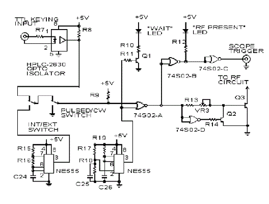
Keying Schematic
A better copy of the schematic saved in different formats can be downloaded for viewing and printing using different software.
A word of warning, if you download one of these other schematic files, be sure to save them with the proper 3 letter extention. The program may assign a different extention so be sure to change it to the proper one!!
KEYSCH.DXF this is a somewhat universal exchange format that can be read by a number of graphics
programs.
KEYSCH.SKD this is the original drawing file in AutoSketch format
If no electronic on-off keying is required (i.e. most guiding experiments), this circuit may be eliminated. In that case, simply tie the tube cathodes to ground.
NOTE: This schematic has continued to evolve as our needs and experience changes. The current schematic is somewhat different than the schematic from the original article. This design requires a single power supply rail ( +5Vdc only) plus fewer components, but provides the ability to adjust only the rise time of the RF. This circuit, along with the +5V power supply are mounted on a small hand wired circuit board.
Unless otherwise specified all resistors are 1/4 watt, 5%, carbon composition resistors
R7 = 220 ohm
R8 = 1.8 K
R9 = 3.3 K
R10 = 470 ohm
R11 = 10 K
R12 = 470 ohm
R13 = 2.7 K
R14 = 1 K
R15 = 2.2 K
R16 = 30 K
R17 = 1.1 K
R18 = 56 K
R19 = 39 K
All capacitors are polarized, 10 V or greater tantalum or electrolytic. Except for C25, they affect the timing of the keying circuit and the delay for allowing filament warm-up, the values are not critical. The values shown give a filament warm-up time of about 20 seconds and an internally generated on-off key rate of about 10 Hz.
C24 = 2.2 uF (affects the pulse rate)
C25 = 1 uF (circuit element that forces the filament timer to restart each time the
power is turned on, use as near 1 uF as you have available)
C26 = 220 uF (affects filament warm up time to extend the life of the tubes)
74S02 is a standard TTL logic gate, however, the 'S' series is very fast and should be used when the fastest rise time is desired. The more common 'LS' will result in a slower rise time.
The HPLC-2630 is a very fast opto-isolator used to receive the TTL keying signal. The more common opto-isolators are much slower and will result in not only a longer delay from receiving the key signal to activation of the RF but also will result in much more jitter in the timing. It is highly recommended that the HPLC-2630 or and equivalent high speed opto-isolator be used. If there is no danger of introducing a ground loop, the opto-isolator could be eliminated. We used it go help prevent ground loop problems.
NE-555 is the standard 555 timer chip. Nothing special here. The circuit on the left generates the pulses and if extremely stable timing is required, C24 should be a capacitor with a low temperature coefficient.
CIRCUIT DESCRIPTION
This circuit provides the following three functions:
- It automatically prevents keying the RF till the tubes filaments have warmed up. This extends the life of the tubes.
- It has control switches that allow the RF to be always off, always on (CW) or to be keyed on and off either with an internally generated signal or from an external TTL source.
- It allows the rise time of the RF to be adjusted.
- It provides a scope trigger signal to trigger an oscilloscope on the keying signal.
Q3 is a high voltage transistor that is connected to the cathodes of the RF tubes. When the transistor is on, the cathodes are effectively grounded and RF is generated. The transistor is turned on by the output of 74S02-A which connect to the base by way of R13 and VR3. These resistors affect the rise time of the current applied to the base of Q3, thus they affect the turn on time of the transistor. This in turn affects the keying envelope of the RF. Adjusting VR3 increases or decreases the rise time.
The output of 74S02-A also drives 74S02-B which turns on a front panel LED to indicate that RF is present and this in turn drives 74S02-C which connects to a front panel BNC connector to provide a trigger signal for an oscilloscope to trigger the scope on the keying signal.
Connected to the base of Q3 is Q2. This transistor is turned on when Q3 is turned off. The purpose of Q2 is to drain the charge from the base of Q3, thus forcing Q3 to turn off more rapidly.
The main keying gate, the 74S02-A, is held off by one of its inputs coming from the right 555 timer IC which is wired as a monostable multivibrator (a one-shot). When power is first applied, the output of the 555 goes high and stays high for about 20 seconds. This high forces the output of 7402-A low and thus Q3 off and prevents the tubes from oscillating. This is to help extend the life of the tubes. After about 20 seconds, the 555 output goes low and 74S02-A is enabled. The other input to 74S02-A is from the front panel key source select switches. They route the various key signals. If the right switch is down (grounded) the output of the gate will be high and thus Q3 will be turned on and RF will be present. If the switch is in the middle position, the input to the gate will be pulled high by R9 and its output will go low, thus Q3 will be off and no RF will be present. If the switch is up, the keying signal will be selected by the left switch. It that switch is down, the keying signal will come from the second 555 timer IC which is wired as an astable multivibrator (an oscillator). This generates a 10 Hz square wave which turns on and off the RF at a 10 Hz rate. If the switch is up, the keying signal comes from the output of an opto-isolator. The input to the opto-isolator is from an external TTL signal. It is coupled to the opto-isolator to help prevent ground loops that may be caused by connecting the ground of the generator with the ground of the TTL signal source. If no TTL signal is present, the input to 74S02-A will be high, thus its output low and no RF will be present. A TTL high will turn on the RF.
Circuit layout is not critical other than that Q2 should be mounted near Q3. Q3 is a high voltage transistor and must be mounted on the chassis. It does not require any extra heat sinking since this generator does not produce much power. There will be high voltage present on the transistor and proper insulators must be used.
Connect the emitter to ground as near the transistor as possible and connect the cathodes to the collector with as short and straight wires as possible.
Not shown is the 5V power supply. This circuits runs on a 5V supply of standard design. Since it requires very little current, a 7805 three terminal regulator provides more than enough current and regulation. The 6.3 VAC filament transformer is used to power the power supply.
Links to:
RF section schematics and description